- 您现在的位置:买卖IC网 > Sheet目录470 > MAX11014BGTM+T (Maxim Integrated)IC RF MESFET AMP 48-TQFN-EP
�� �
�
�Automatic� RF� MESFET� Amplifier�
�Drain-Current� Controllers�
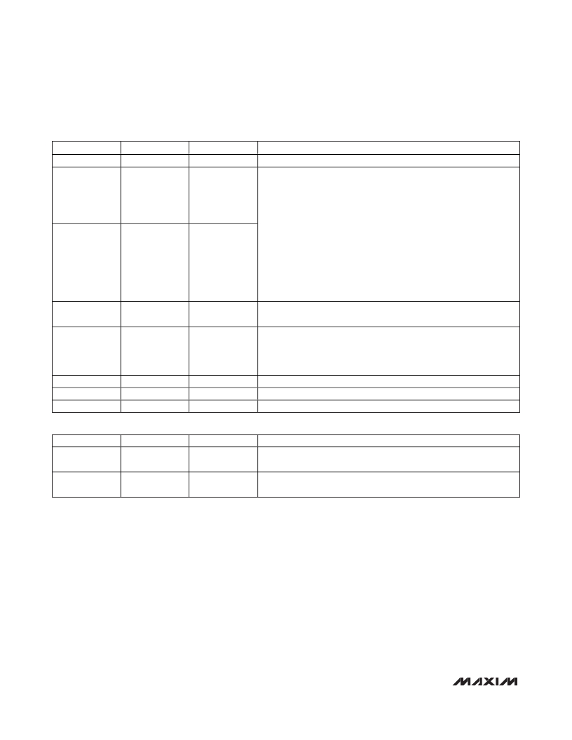
�Table� 22.� SCLR� (Write)�
�BIT� NAME�
�X�
�DATA� BIT�
�D15–D7�
�RESET� STATE�
�X�
�Don’t� care.�
�FUNCTION�
�Write� the� following� sequence� to� perform� a� full� reset� and� return� all� internal�
�registers� to� their� respective� reset� state:�
�FULLRESET�
�D6�
�N/A�
�Write� to� the� software� clear� register� once� with� FULLRESET� =� 0� and�
�ARMRESET� =� 1.� Write� a� second� word� to� the� software� clear� register� with�
�FULLRESET� =� 1� and� ARMRESET� =� 0.�
�The� full� reset� takes� effect� after� completion� of� the� second� write� to� this�
�register.�
�After� a� full� software� reset,� the� internal� registers� return� to� their� power-on�
�state,� but� the� internal� oscillator� remains� running� (unlike� at� power-up).�
�ARMRESET�
�D5�
�0�
�After� a� full� software� reset,� it� is� not� necessary� to� set� the� FULLPD� bit� to� 0�
�(as� it� is� on� a� normal� power-on� reset)� before� attempting� any� other�
�commands.� The� BUSY� output� is� set� high� and� the� ALU� initializes� internal�
�RAM� before� setting� BUSY� low.�
�ALMSCLR�
�D4�
�N/A�
�Set� to� 1� to� reset� all� ALARM� threshold� registers� and� the� ALARM� flag�
�register.�
�Set� to� 1� to� force� the� ALU� to� clear� the� pointers� and� lookup� value� cache� to�
�CACHECLR�
�D3�
�N/A�
�their� power-up� values.� This� forces� an� LUT� operation� and� a� V� DAC(CODE)�
�calculation� for� the� next� sample,� regardless� of� whether� the� sample�
�produces� a� table� pointer� that� is� different.�
�FIFOCLR�
�DAC2CLR�
�DAC1CLR�
�D2�
�D1�
�D0�
�N/A�
�N/A�
�N/A�
�Set� to� 1� to� reset� the� FIFO� address� pointers� and� clear� the� FIFO’s� contents.�
�Set� to� 1� to� reset� the� channel� 2� DAC� input� and� output� registers.�
�Set� to� 1� to� reset� the� channel� 1� DAC� input� and� output� registers.�
�Table� 23.� LUTADD� (Write)�
�BIT� NAME�
�LUTWORD7–�
�LUTWORD0�
�LUTADD7–�
�LUTADD0�
�DATA� BIT�
�D15–D8�
�D7–D0�
�RESET� STATE�
�0000� 0000�
�0000� 0000�
�FUNCTION�
�Set� these� 8� bits� to� determine� the� number� of� LUT� words� to� be�
�read/written.�
�Set� these� 8� bits� to� determine� the� base� address� for� the� read/write�
�operation.�
�SCLR� (Write)�
�write� to� this� register.�
�Write� to� the� software� clear� register� to� reset� all� of� the�
�internal� registers,� clear� the� internal� ALU� or� reset� the� FIFO�
�pointers� and� clear� the� FIFO.� This� register� also� resets� the�
�ALARM� threshold� registers,� ALARM� flag� register� and� the�
�?�
�It� is� recommended� a� FULLRESET� be� completed� after�
�power-up.� See� Appendix:� Startup� Code� Example� for�
�sample� startup� code.�
�DAC� registers.� Set� the� command� byte� to� 74h� to� write� to�
�the� software� clear� register.� See� Table� 22.� Bits� D15–D7�
�are� don’t� care.� The� FULLRESET� bit,� D6,� and� ARMRESET�
�bit,� D5,� provide� functionality� for� a� full� reset.� Write� the�
�following� sequence� to� perform� a� full� reset� and� return� all�
�internal� register� bits� to� their� respective� reset� state:�
�?� Write� to� the� software� clear� register� once� with�
�FULLRESET� =� 0� and� ARMRESET� =� 1.�
�?� Write� a� second� word� to� the� software� clear� register�
�with� FULLRESET� =� 1� and� ARMRESET� =� 0.� The� full�
�reset� takes� effect� after� completion� of� the� second�
�Set� the� ALMSCLR� bit,� D4,� to� 1� to� reset� all� ALARM� thresh-�
�old� register� bits� and� the� ALARM� flag� register� bits.� Set� the�
�CACHECLR� bit,� D3,� to� 1� to� force� the� ALU� to� clear� the�
�pointers� and� lookup� value� cache� to� their� power-up� val-�
�ues.� This� forces� a� LUT� operation� and� a� V� DAC(CODE)� cal-�
�culation� for� the� next� sample,� regardless� of� whether� the�
�sample� produces� a� table� pointer� that� is� different.� Set� the�
�FIFOCLR� bit,� D2,� to� 1,� reset� the� FIFO� address� pointers,�
�and� clear� the� FIFO’s� contents.� Set� the� DAC2CLR� bit,� D1,�
�to� 1� to� reset� the� channel� 2� DAC� input� and� output� register�
�bits.� Set� the� DAC1CLR� bit,� D0,� to� 1� to� reset� the� channel� 1�
�DAC� input� and� output� register� bits.�
�48�
�______________________________________________________________________________________�
�发布紧急采购,3分钟左右您将得到回复。
相关PDF资料
MAX12000ETB+T
IC AMP GPS FRONT 1575MHZ 10TDFN
MAX12005ETM+T
IC SATELLITE IF SWITCH 48-TQFN
MAX1385BUTM+
IC RF LDMOS BIAS CNTRLR 48-TQFN
MAX1470EUI+T
IC RECEIVER 315MHZ 28-TSSOP
MAX1470EVKIT-315
EVAL KIT FOR MAX1470 315MHZ
MAX1471EVKIT-315
EVAL KIT FOR MAX1471 315MHZ
MAX1472EVKIT-433#
EVAL KIT MAX1472
MAX1473EVKIT-433
EVAL KIT MAX1473
相关代理商/技术参数
MAX11014EVKIT+
制造商:Maxim Integrated Products 功能描述:EVALUATION KIT FOR THE MAX11014 - Bulk
MAX11015
功能描述:射频放大器
RoHS:否 制造商:Skyworks Solutions, Inc. 类型:Low Noise Amplifier 工作频率:2.3 GHz to 2.8 GHz P1dB:18.5 dBm 输出截获点:37.5 dBm 功率增益类型:32 dB 噪声系数:0.85 dB 工作电源电压:5 V 电源电流:125 mA 测试频率:2.6 GHz 最大工作温度:+ 85 C 安装风格:SMD/SMT 封装 / 箱体:QFN-16 封装:Reel
MAX11015BGTM
制造商:MAXIM 制造商全称:Maxim Integrated Products 功能描述:Automatic RF MESFET Amplifier Drain-Current Controllers
MAX11015BGTM+
制造商:MAXIM 制造商全称:Maxim Integrated Products 功能描述:Automatic RF MESFET Amplifier Drain-Current Controllers
MAX11017
功能描述:模数转换器 - ADC
RoHS:否 制造商:Texas Instruments 通道数量:2 结构:Sigma-Delta 转换速率:125 SPs to 8 KSPs 分辨率:24 bit 输入类型:Differential 信噪比:107 dB 接口类型:SPI 工作电源电压:1.7 V to 3.6 V, 2.7 V to 5.25 V 最大工作温度:+ 85 C 安装风格:SMD/SMT 封装 / 箱体:VQFN-32
MAX11017ATL+
功能描述:模数转换器 - ADC
RoHS:否 制造商:Texas Instruments 通道数量:2 结构:Sigma-Delta 转换速率:125 SPs to 8 KSPs 分辨率:24 bit 输入类型:Differential 信噪比:107 dB 接口类型:SPI 工作电源电压:1.7 V to 3.6 V, 2.7 V to 5.25 V 最大工作温度:+ 85 C 安装风格:SMD/SMT 封装 / 箱体:VQFN-32
MAX11017ETL+
功能描述:模数转换器 - ADC
RoHS:否 制造商:Texas Instruments 通道数量:2 结构:Sigma-Delta 转换速率:125 SPs to 8 KSPs 分辨率:24 bit 输入类型:Differential 信噪比:107 dB 接口类型:SPI 工作电源电压:1.7 V to 3.6 V, 2.7 V to 5.25 V 最大工作温度:+ 85 C 安装风格:SMD/SMT 封装 / 箱体:VQFN-32
MAX11019
功能描述:模数转换器 - ADC
RoHS:否 制造商:Texas Instruments 通道数量:2 结构:Sigma-Delta 转换速率:125 SPs to 8 KSPs 分辨率:24 bit 输入类型:Differential 信噪比:107 dB 接口类型:SPI 工作电源电压:1.7 V to 3.6 V, 2.7 V to 5.25 V 最大工作温度:+ 85 C 安装风格:SMD/SMT 封装 / 箱体:VQFN-32